Combinational Circuits: Multiplexers, Decoders, and Encoders
Learning Objectives
By the end of this lesson, you should be able to:
- explain what makes a circuit combinational rather than sequential;
- design small multiplexers, demultiplexers, decoders, and encoders from truth tables;
- calculate the number of select, input, and output lines;
- recognize propagation delay and enable polarity issues;
- choose common 74HC logic ICs for practical designs;
- verify a combinational circuit with static and dynamic tests.
What Is a Combinational Circuit?
A combinational circuit has no memory. Its output depends only on the present input values.
There is still a real delay through the gates. The output changes after the longest input-to-output path settles.
total propagation delay is approximately the sum of delays on the critical path
Sequential circuits, covered in the next lessons, include memory elements such as latches or flip-flops. A combinational block should not depend on previous input history.
Design Flow
Use this repeatable process:
- Write the exact input and output meaning.
- Build a truth table.
- Derive Boolean expressions.
- Simplify if useful.
- Draw or code the implementation.
- Verify all input combinations and timing assumptions.
Multiplexer: Many Inputs to One Output
A multiplexer, or MUX, selects one of several data inputs and forwards it to one output.
For a power-of-two MUX:
number of data inputs = 2^select_lines
select_lines = log2(data_inputs)
| Data inputs | Select lines |
|---|---|
| 2 | 1 |
| 4 | 2 |
| 8 | 3 |
| 16 | 4 |
2:1 MUX
Truth table:
| S | Y |
|---|---|
| 0 | I0 |
| 1 | I1 |
Boolean expression:
Y = S' I0 + S I1

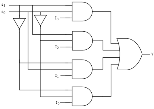
4:1 MUX
Truth table:
| S1 | S0 | Y |
|---|---|---|
| 0 | 0 | I0 |
| 0 | 1 | I1 |
| 1 | 0 | I2 |
| 1 | 1 | I3 |
Expression:
Y = S1' S0' I0 + S1' S0 I1 + S1 S0' I2 + S1 S0 I3
MUX as a Logic Function Generator
A MUX can implement a Boolean function by using function variables as select lines and wiring data inputs to constants or signals.
Example: implement XOR with a 4:1 MUX.
| A | B | A xor B | MUX input |
|---|---|---|---|
| 0 | 0 | 0 | I0 = 0 |
| 0 | 1 | 1 | I1 = 1 |
| 1 | 0 | 1 | I2 = 1 |
| 1 | 1 | 0 | I3 = 0 |
Connect A and B to the select pins, then wire I0=0, I1=1, I2=1, and I3=0.
Demultiplexer: One Input to Many Outputs
A demultiplexer routes one input to one selected output.
For a 1:4 DEMUX:
| S1 | S0 | Y0 | Y1 | Y2 | Y3 |
|---|---|---|---|---|---|
| 0 | 0 | I | 0 | 0 | 0 |
| 0 | 1 | 0 | I | 0 | 0 |
| 1 | 0 | 0 | 0 | I | 0 |
| 1 | 1 | 0 | 0 | 0 | I |
Expressions:
Y0 = S1' S0' I
Y1 = S1' S0  I
Y2 = S1  S0' I
Y3 = S1  S0  I
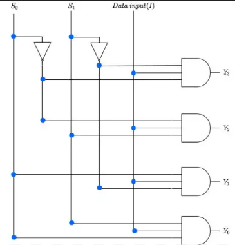
Demultiplexers are used for signal routing, LED matrix scanning, address selection, and simple serial-to-parallel distribution.
Decoder: Binary Code to One-Hot Output
A decoder activates one output line for each binary input code.
For an enabled 2-to-4 decoder:
| EN | A1 | A0 | Y0 | Y1 | Y2 | Y3 |
|---|---|---|---|---|---|---|
| 0 | X | X | 0 | 0 | 0 | 0 |
| 1 | 0 | 0 | 1 | 0 | 0 | 0 |
| 1 | 0 | 1 | 0 | 1 | 0 | 0 |
| 1 | 1 | 0 | 0 | 0 | 1 | 0 |
| 1 | 1 | 1 | 0 | 0 | 0 | 1 |
Expressions:
Y0 = EN A1' A0'
Y1 = EN A1' A0
Y2 = EN A1  A0'
Y3 = EN A1  A0
Decoders are common in memory address selection, chip-select generation, seven-segment display logic, and instruction decoding.
Encoder: One-Hot Input to Binary Code
An encoder converts one active input line into a binary code.
For a simple 4-to-2 encoder:
| I3 | I2 | I1 | I0 | A1 | A0 |
|---|---|---|---|---|---|
| 0 | 0 | 0 | 1 | 0 | 0 |
| 0 | 0 | 1 | 0 | 0 | 1 |
| 0 | 1 | 0 | 0 | 1 | 0 |
| 1 | 0 | 0 | 0 | 1 | 1 |
This assumes exactly one input is active. If two inputs can be active together, use a priority encoder.
Priority Encoder
A priority encoder chooses the highest-priority active input.
Example priority: I3 highest, I0 lowest.
| I3 | I2 | I1 | I0 | A1 | A0 | Valid |
|---|---|---|---|---|---|---|
| 1 | X | X | X | 1 | 1 | 1 |
| 0 | 1 | X | X | 1 | 0 | 1 |
| 0 | 0 | 1 | X | 0 | 1 | 1 |
| 0 | 0 | 0 | 1 | 0 | 0 | 1 |
| 0 | 0 | 0 | 0 | 0 | 0 | 0 |
Priority encoders are used in interrupt controllers, keyboard scanners, and event selection logic.
Worked Example: Address Decode
Problem: A microcontroller has four external devices. Use address bits A1:A0 to generate active-high chip-selects CS0 to CS3.
Solution: Use a 2-to-4 decoder.
CS0 = A1' A0'
CS1 = A1' A0
CS2 = A1  A0'
CS3 = A1  A0
Verification table:
| A1 | A0 | CS0 | CS1 | CS2 | CS3 |
|---|---|---|---|---|---|
| 0 | 0 | 1 | 0 | 0 | 0 |
| 0 | 1 | 0 | 1 | 0 | 0 |
| 1 | 0 | 0 | 0 | 1 | 0 |
| 1 | 1 | 0 | 0 | 0 | 1 |
Only one chip-select is active for each address. That one-hot property is the key safety check.
Timing and Glitches
Even a combinational circuit can briefly glitch when inputs change because different gate paths have different delays.
title "Illustrative decoder skew"
time start=0 end=40 unit=ns divisions=8

A0: square label="A0" low=0 high=1 duty=50 cycles=1 unit=V color=#2563eb
A1: step label="A1" low=0 high=1 at=20 unit=V color=#16a34a
Y: pulse label="Brief wrong select" low=0 high=1 at=20 width=3 unit=logic color=#dc2626
marker CHANGE at=20 label="inputs change"
The waveform is an explanatory timing sketch, not a measured simulation. In real systems, latch or register decoder outputs when glitches could enable two devices or create an unsafe pulse.
Common ICs
| Function | Example IC | Notes |
|---|---|---|
| Quad 2:1 MUX | 74HC157 | common data selector |
| 8:1 MUX | 74HC151 | one output selected from 8 inputs |
| Analog MUX | CD4051 | routes analog signals within limits |
| 3-to-8 decoder | 74HC138 | active-low outputs and enables |
| 4-to-16 decoder | 74HC154 | active-low outputs |
| Priority encoder | 74HC148 | active-low inputs and outputs |
Always check the datasheet polarity. Many classic decoder and encoder ICs use active-low enables or active-low outputs.
Practical Verification Checklist
- Verify every truth-table row.
- Confirm no more than one one-hot output can be active.
- Check active-high versus active-low names and bubbles.
- Calculate the critical-path delay from datasheet values.
- For chip-selects, check that glitches cannot enable two devices.
- Tie unused inputs to a valid logic level.
- Add decoupling capacitors near logic IC supply pins.
Common Mistakes
| Mistake | Symptom | Debug step |
|---|---|---|
| Wrong select-bit order | MUX picks the wrong input | Label whether S0 is LSB |
| Ignoring enable polarity | Circuit appears always disabled | Check datasheet truth table |
| Multiple encoder inputs active | Output code is ambiguous | Use a priority encoder or valid flag |
| Treating analog MUX as ideal | Signal clips or leaks | Check supply range, on-resistance, leakage |
| No glitch analysis | False chip-select pulse | Register the output or redesign timing |
Summary
Multiplexers select one of many inputs. Demultiplexers route one input to one of many outputs. Decoders convert binary codes into one-hot outputs, and encoders convert one-hot inputs into binary codes. All are combinational, so correctness comes from truth tables, Boolean expressions, polarity checks, and propagation-delay verification.
Further Reading
- Texas Instruments, Logic Guide
- Nexperia datasheets for 74HC138, 74HC151, 74HC157, and 74HC148
- M. Morris Mano and Michael Ciletti, Digital Design
- Stephen Brown and Zvonko Vranesic, Fundamentals of Digital Logic with Verilog Design